(Hong Kong)


Product Summary
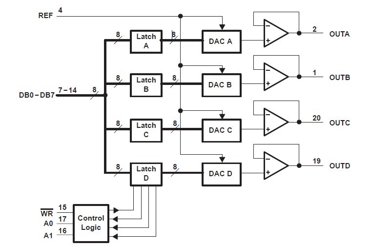
The TLC7226CDWR consists of four 8-bit voltage-output digital-to-analog converters (DACs), with output buffer amplifiers and interface logic with double register-buffering. Separate on-chip latches are provided for each of the DACs. Data is transferred into one of these data latches through a common 8-bit TTL/CMOS-compatible (5 V) input port. Control inputs A0 and A1 determine which DAC is loaded when WR goes low. Only the data held in the DAC registers determines the analog outputs of the converters. The double register buffering allows simultaneous update of all four outputs under control of LDAC. All logic inputs are TTL- and CMOS-level compatible and the control logic is speed compatible with most 8-bit microprocessors. Each DAC includes an output buffer amplifier capable of driving up to 5 mA of output current. The TLC7226CDWR performance is specified for input reference voltages from 2 V to VDD - 4 V with dual supplies. The voltage-mode configuration of the DACs allow the TLC7226CDWR to be operated from a single power-supply rail at a reference of 10 V. The TLC7226CDWR is fabricated in a LinBiCMOS. process that has been specifically developed to allow high-speed digital logic circuits and precision analog circuits to be integrated on the same chip. The TLC7226CDWR has a common 8-bit data bus with individual DAC latches. This provides a versatile control architecture for simple interface to microprocessors. All latch-enable signals are level triggered. Combining four DACs, four operational amplifiers, and interface logic into a small, 0.3-inch wide, 24-terminal SOIC allows significant reduction in board space requirements and offers increased reliability in systems using multiple converters. The pinout optimizes board layout with all of the analog inputs and outputs at one end of the package and all of the digital inputs at the other. The TLC7226CDWR is characterized for operation from 0℃ to 70℃. The TLC7226CDWR is characterized for operation from -25℃to 85℃.
Parametrics
TLC7226CDWR absolute maximum ratings: (1)Supply voltage range, VDD: to AGND or DGND: -0.3 V to 17 V; (2)to VSS: -0.3 V to 24 V; (3)Supply voltage range, VSS: to AGND or DGND: -7 V to VDD; (4)Voltage range between AGND and DGND:-0.3 V to VDD; (5)Input voltage range, VI (to DGND): -0.3 V to VDD + 0.3 V; (6)Reference voltage range, Vref (to AGND): -0.3 V to VDD; (7)Output voltage range, VO (to AGND): VSS to VDD; (8)Continuous total power dissipation at (or below) TA = 25℃ : 500 mW; (9)Operating free-air temperature range: C suffix: 0℃ to 70℃; (10)I suffix : -40℃ to 85℃; (11)Storage temperature range, Tstg: -65℃ to 150℃; (12)Lead temperature 1,6 mm (1/16 inch) from case for 10 seconds: 260℃.
Features
TLC7226CDWR features: (1)Four 8-Bit D/A Converters With Individual References; (2)Direct Bipolar Operation Without an External Level-Shift Amplifier; (3)Microprocessor Compatible; (4)TTL/CMOS Compatible; (5)Single Supply Operation Possible; (6)Simultaneous Update Facility; (7)Binary Input Coding.
Diagrams
| Image | Part No | Mfg | Description |  |
Pricing (USD) |
Quantity | ||||||||
|---|---|---|---|---|---|---|---|---|---|---|---|---|---|---|
 |
 TLC7226CDWR |
Texas Instruments |
DAC (D/A Converters) Quad Parallel-In Sngl/Dual Sply |
Data Sheet |
|
|
||||||||
|
TLC7226CDWRG4 |
Texas Instruments |
DAC (D/A Converters) Quad Parallel-In Sngl/Dual Sply |
Data Sheet |
|
|
||||||||