(Hong Kong)

Product Summary
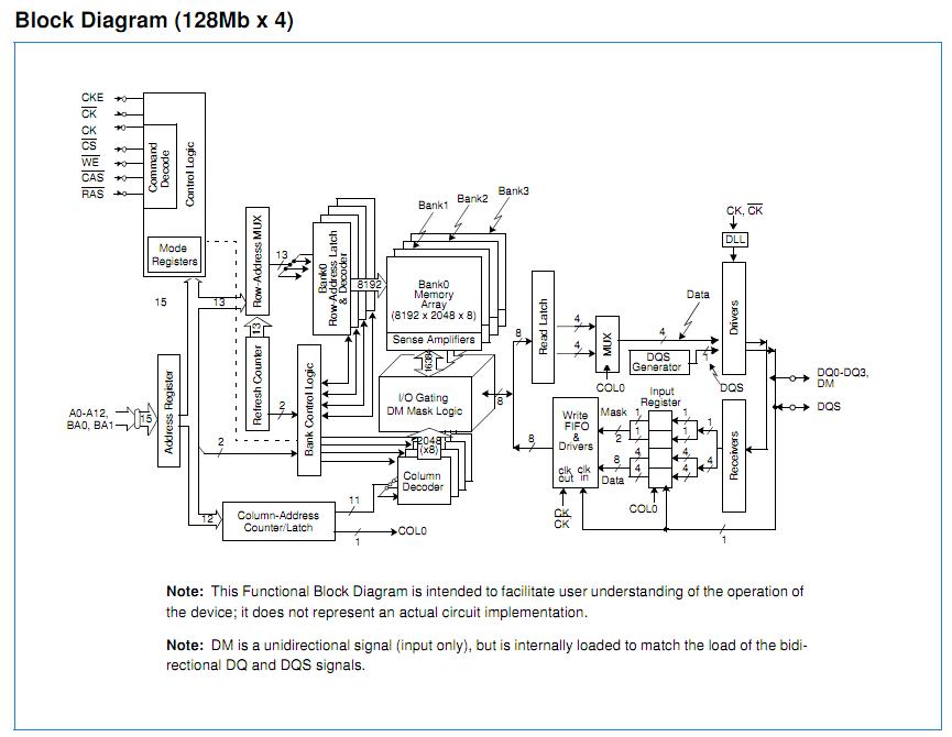
The NT5DS32M16BS-5T is a high-speed CMOS, dynamic random-access memory containing 536,870,912 bits. It is internally configured as a quad-bank DRAM.The NT5DS32M16BS-5T uses a double-data-rate architec-ture to achieve high-speed operation. The double data rate architecture is essentially a 2n prefetch architecture with an interface designed to transfer two data words per clock cycle at the I/O pins. A single read or write access for the 512Mb DDR SDRAM effectively consists of a single 2n-bit wide, one clock cycle data transfer at the internal DRAM core and two corresponding n-bit wide, one-half-clock-cycle data transfers at the I/O pins.
Parametrics
NT5DS32M16BS-5T absolute maximum ratings: (1)VIN, VOUT Voltage on I/O pins relative to VSS: -0.5 to VDDQ+ 0.5 V; (2)VIN Voltage on Inputs relative to VSS: -0.5 to +3.6 V; (3)VDD Voltage on VDD supply relative to VSS: -0.5 to +3.6 V; (4)VDDQ Voltage on VDDQ supply relative to VSS: -0.5 to +3.6 V; (5)TA Operating Temperature (Ambient): 0 to +70℃; (6)TSTG Storage Temperature (Plastic): -55 to +150℃; (7)PD Power Dissipation: 1.0 W; (8)IOUT Short Circuit Output Current: 50 mA.
Features
NT5DS32M16BS-5T features: (1)DDR 512M bit, die B, based on 110nm design rules; (2)Double data rate architecture: two data transfers per clock cycle; (3)Bidirectional data strobe (DQS) is transmitted and received with data, to be used in capturing data at the receiver; (4)DQS is edge-aligned with data for reads and is center-aligned with data for writes; (5)Differential clock inputs (CK and CK); (6)Four internal banks for concurrent operation; (7)Data mask (DM) for write data; (8)DLL aligns DQ and DQS transitions with CK transitions; (9)Commands entered on each positive CK edge; data and data mask referenced to both edges of DQS; (10)Burst lengths: 2, 4, or 8; (11)CAS Latency: 2 / 2.5 (6K & 75B), 2.5 / 3 (6K & 5T); (12)Auto Precharge option for each burst access; (13)Auto Refresh and Self Refresh Modes; (14)7.8ms Maximum Average Periodic Refresh Interval; (15)2.5V (SSTL_2 compatible) I/O; (16)VDD = VDDQ = 2.5V ± 0.2V (6K & 75B); (17)VDD = VDDQ = 2.6V ± 0.1V (5T).
Diagrams
 |
 NT5DS128M4BF |
Other |
|
Data Sheet |
Negotiable |
|
||||
|
NT5DS128M4BT |
Other |
|
Data Sheet |
Negotiable |
|
||||
|
NT5DS32M16BF |
Other |
|
Data Sheet |
Negotiable |
|
||||
|
NT5DS32M16BG-6K |
Other |
|
Data Sheet |
Negotiable |
|
||||
|
NT5DS32M16BT |
Other |
|
Data Sheet |
Negotiable |
|
||||
|
NT5DS32M8AT |
Other |
|
Data Sheet |
Negotiable |
|
||||