(Hong Kong)

Product Summary
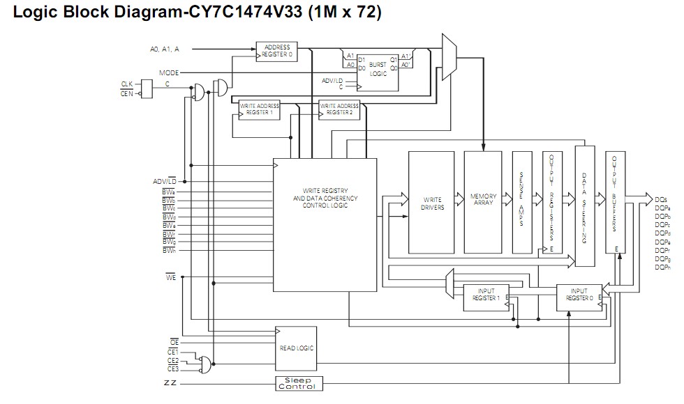
The CY7C1474V33-167BGC is a 1M x 72 Synchronous pipelined burst SRAM with No Bus Latency (NoBL) logic. The CY7C1474V33-167BGC is designed to support unlimited true back-to-back Read/Write operations with no wait states. The CY7C1474V33-167BGC is equipped with the advanced (NoBL) logic required to enable consecutive Read/Write operations with data being transferred on every clock cycle. This feature dramatically improves the throughput of data in systems that require frequent Write/Read transitions. The CY7C1474V33-167BGC is pin compatible and functionally equivalent to ZBT device.
Parametrics
CY7C1474V33-167BGC absolute maximum ratings: (1)Storage Temperature:–65 to +150℃; (2)Ambient Temperature with Power Applied:–55 to +125℃; (3)Supply Voltage on VDD Relative to GND:–0.5V to +4.6V; (4)DC to Outputs in Tri-State:–0.5V to VDDQ + 0.5V; (5)DC Input Voltage:–0.5V to VDD + 0.5V; (6)Current into Outputs (LOW): 20 mA; (7)Static Discharge Voltage(per MIL-STD-883, Method 3015): > 2001V; (8)Latch-up Current: > 200 mA.
Features
CY7C1474V33-167BGC features: (1)Pin-compatible and functionally equivalent to ZBT; (2)Supports 250-MHz bus operations with zero wait states; (3)Internally self-timed output buffer control to eliminate the need to use asynchronous OE; (4)Fully registered (inputs and outputs) for pipelined operation; (5)Byte Write capability; (6)Single 3.3V power supply; (7)3.3V/2.5V I/O power supply; (8)Clock Enable (CEN) pin to suspend operation; (9)Synchronous self-timed writes; (10)IEEE 1149.1 JTAG Boundary Scan compatible; (11)Burst capability—linear or interleaved burst order.
Diagrams
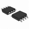
| Image | Part No | Mfg | Description |  |
Pricing (USD) |
Quantity | ||||||
|---|---|---|---|---|---|---|---|---|---|---|---|---|
 |
 CY7C1474V33-167BGC |
Cypress Semiconductor |
SRAM 1Mx72 3.3V NoBL PL SRAM COM |
Data Sheet |
|
|
||||||
|
CY7C1474V33-167BGCT |
Cypress Semiconductor |
SRAM 1Mx72 3.3V NoBL PL SRAM COM |
Data Sheet |
Negotiable |
|
||||||